
140W power supply exploits GaN switches for efficiency gains
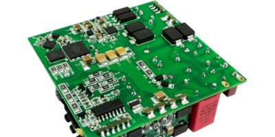
Innoscience has announced a high density 140W power supply demo that uses the company’s high and low voltage GaN HEMT (high electron mobility transistor) devices. It achieves efficiencies of over 95 per cent (230V AC, 5V / 28A) in a form factor of 60 x 60 x 22mm (2.4 x 2.4 x 0.9 inch).
The 140W 300kHz AC/DC adapter uses a CRM Totem Pole power factor correction (PFC) with asymmetrical half bridge (AHB) topology. It features Innoscience’s INN650DA140A, a 650V /140mΩ GaN HEMT in the 5.0 x 6.0mm DFN package, for switches S1 and S2, the 650V / 240 mOhm, 8.0 x 8.0mm DFN packaged INN650D240A for S3 and the INN650DA240A, a 5.0 x 6.0mm DFN 650V / 240 mOhm device for S4. The S5 and S6 switches are delivered by the INN150LA070A, a 150V / 7 mOhm, 2.2 x 3.2mm LGA part within Innoscience’s low-voltage GaN HEMT range.
Innoscience said it is the only company which can mass produce both high- and low-voltage eight-inch GaN-on-Si devices. According to the company, the power supply has a class-leading power density of 1.76W/cm3 (29W/in3).
Dr Denis Marcon, general manager of Innoscience Europe and marketing manager for the USA and Europe, explained: “By using GaN switches for both the high- and low-voltage functions on this design, we are maximisng efficiency rather than compromising it with lossy silicon devices. . . thanks to Innoscience’s cost-effective and high-volume manufacturing processes and capabilities.”
The design targets SB PD3.1 notebooks and power tools, said Yi Sun, general manager of Innoscience America and senior vice president of Product and Engineering. “This design . . . is a full two per cent more efficient than silicon designs; this proves what can be achieved if GaN FETs are used everywhere, even in a relatively simple design,” he said.
Founded in December 2015, Innoscience is the only IDM (integrated device manufacturer) that can mass-produce both high- and low-voltage GaN devices. Innoscience has its own normally-off, single-die technology and claims to have the industry’s largest eight-inch wafer GaN-on-Si production capacity. In the consumer market, fast charging products have led the adoption of GaN technology. Today, many other markets are also starting to use GaN, said Innoscience.

