
Intel achieves 90 per cent cell use in power chip fabrication
Intel has announced it has implemented reverse or backside power in a product-like chip, resulting in over 90 per cent cell utilisation. The company will present two papers at the VLSI Symposium in Kyoto, Japan (11 to 16 June).
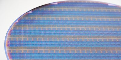
The company has published results of a production test for the PowerVia backside power technology which is expected to be available next year as part of the Intel 20A manufacturing node. The production test is the next step in what is believed to be the first implementation of backside power in silicon, solving decades of interconnect bottlenecks in areas scaling by moving power routing to the back of a wafer.
“PowerVia is a major milestone in our aggressive ‘five nodes in four years’ strategy and on our path to achieving a trillion transistors in a package in 2030,” said Ben Sell, Intel’s vice president of technology development.
The company used a trial process node and subsequent test chip to de-risk backside power for its leading process nodes, he confirmed.
PowerVia was tested on its own internal test node to debug and ensure good functionality of the technology before its integration with RibbonFET in Intel 20A. After fabrication and testing on a silicon test chip, PowerVia was confirmed to bring efficient use of chip resources with greater than 90 per cent cell utilisation and major transistor scaling for performance and efficiency gains in end products.
Surging use cases, including AI and graphics, require smaller, denser and more powerful transistors to meet growing computing demands. Power and signal lines within a transistor’s architecture have competed for the same resources but separating the two could enable chips to increase performance and energy efficiency. Backside power delivery is vital to transistor scaling, enabling chip designers to increase transistor density without sacrificing resources to deliver more power and performance than ever, said Intel.
Intel 20A and Intel 18A will introduce both PowerVia backside power technology and RibbonFET gate-all-around technology. These provide a completely new way of delivering power to the transistors, challenging thermal and debugging issues. Intel engineers developed mitigation techniques to prevent the thermals from becoming an issue. The debug community also developed new techniques to ensure the new design structure could be appropriately de-bugged. As a result, the test implementation delivered solid yield and reliability metrics while demonstrating the intrinsic value proposition of the technology before it joins new RibbonFET architecture.
The test also leveraged design rules enabled by EUV (extreme ultraviolet) lithography, which produced results including standard cell utilisation of more than 90 per cent over large areas of the die, enabling greater cell density, which can be expected to lower costs. The test also showed more than 30 per cent platform voltage droop improvement and six per cent frequency benefit. Intel also achieved thermal characteristics in the PowerVia test chip in line with higher power densities expected from logic scaling.
In a third paper to be presented during VLSI, Intel technologist Mauro Kobrinsky will explain Intel’s research into more advanced methods to deploy PowerVia, such as enabling both signalling and power delivery on either the front or the back side of the wafer.

