The no-compromise solution
In multisport competitions, most athletes have some weakness in one or the other discipline. However, this is not the case with the new R&S®SMA100 B analog signal generator. With top scores in every aspect, the new signal generator stands alone in front of the competition.
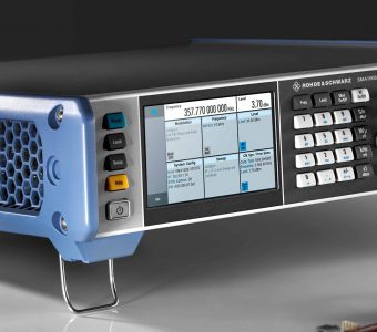
Fig. 1: With the high-end R&S®SMA100 B analog RF and microwave generator, engineers no longer have to compromise between output power and spectral purity.
R&D engineers must often push the limits of what is technically feasible to build a product with the best possible characteristics. In the field of electronics, an analog signal source is commonly the solution of choice for maximizing the potential of a design or verifying its performance. Ideally, this signal source should have sufficiently high performance to avoid influencing the measurement results. For example, engineers who test A/D and D/A converters need signals with the highest possible spurious-free dynamic range (SFDR) as well as the lowest possible wideband noise. For radar engineers, minimal phase noise is the most important requirement. When working with large test setups with high cable losses, the signal source needs high output power to avoid using performance- degrading external amplifiers. Unfortunately, until now, all commercially available signal generators have entailed some sort of compromise; no instrument existed that could simultaneously satisfy all of these criteria.
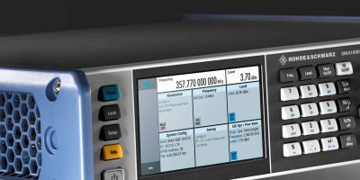
When Rohde & Schwarz decided to develop a successor to its R&S®SMA100 A and R&S®SMF100 A RF and microwave signal generators, it set itself a simple but very ambitious goal: the new instrument should deliver top characteristics – but without any complicated dependencies between them. The result is the R&S®SMA100 B, which combines uncompromisingly high output power with unprecedented signal quality (Figs. 1 and 5).
The following examples illustrate typical applications where the instrument’s strengths come into play.
ADC/DAC component testing
Each new generation of A/D and D/A converters brings higher maximum clock frequencies and higher effective resolution. In order to test such high-performance components, the spectral purity of the source for the clock and test signals must exceed that of the device under test (DUT). The R&S®SMA100 B generates extremely pure signals with SFDR < 100 dBc for a 1 GHz carrier frequency and < 80 dBc for a 10 GHz carrier frequency. This is an improvement of 10 dB to 18 dB over the previous generation of instruments, and also clearly exceeds the specifications of all comparable instruments on the market. As seen in Fig. 2, the measured nonharmonic suppression is well below the guaranteed values.
High sampling frequency and resolution require a signal source with very low wideband noise. The reason is that it takes clock signals with low wideband noise to avoid degrading the signal-to-noise ratio of the ADC’s sampled input signal. This applies especially to ADCs that use under sampling. In the R&S®SMA100 B, an optimized RF design has been combined with a new and fully digital amplitude control loop to ensure typical wideband noise of –160 dBc/Hz for a 10 GHz carrier frequency. Until now, such a value has been attained only by a few very specialize4
signal sources.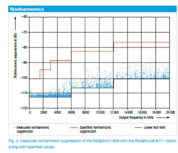
Fig. 2: Measured nonharmonic suppression of the R&S®SMA100 B with the R&S®SMAB-B 711 option along with specified values.
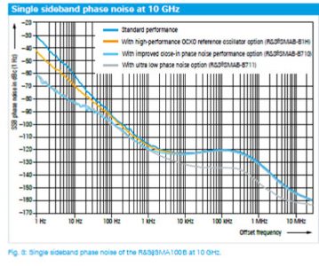
Fig. 3: Single sideband phase noise of the R&S®SMA100 B at 10 GHz.
When testing ADCs, two signal sources are commonly required: the first source delivers the clock for the DUT and the second source delivers the analog input signal. The R&S®SMA100 B has both. The optional clock synthesizer provides a second, fully independent signal source up to 6 GHz with extremely low phase and wideband noise. This option has been optimized for the clock inputs of ADCs. Its frequency can be set independently of the main signal. A common 1 GHz reference is used to achieve very high phase stability between the clock output signal and the main synthesizer signal. In addition, the signal type, amplitude and DC offset can all be set to support common unbalanced and differential clock interfaces.
High-end radar development
When designing and testing high-end radar systems, detection sensitivity is often limited by the phase noise of the RF signal source. The R&S®SMA100 B has multiple options available that can improve the phase noise in order to fulfill even the most demanding requirements (Fig. 3). The close-in phase noise can be as low as typ. –60 dBc/Hz for a 1 Hz offset and 10 GHz carrier frequency. For applications requiring the lowest possible phase noise across the entire offset range, an option with a YIG oscillator is available that can be used to attain a value of –132 dBc/Hz (typ.) for a 10 GHz output frequency at offsets from 10 kHz to 100 kHz. The R&S®SMA100 B is clearly in a league of its own when it comes to phase noise performance.
When testing radar systems, fast and well-controlled RF pulses are essential. With 5 ns (typ.) rise/fall time and better than 80 dB pulse dynamic range, the R&S®SMA100 B is ideal for radar applications. State-of-the-art radar receivers must normally also be tested with very narrow pulses that have high level stability and level repeatability. The pulse modulator in the R&S®SMA100 B was designed especially for this purpose. It can control the amplitudes of pulses down to 100 ns pulse length from the very first pulse on, even in situations with a small duty cycle.
Production testing of microwave amplifiers
When testing power amplifiers, sufficient drive power is crucial. In the past, microwave signal generators were typically unable to produce sufficient drive power on their own and needed costly external amplifiers. The R&S®SMA100 B, however, has built-in power amplifiers, either as standard or optional (Fig. 4). Three output power levels are available. In cases where the standard version is not adequate, a high output power option of up to +35 dBm can be activated with a keycode (no factory service required). The ultra-high output power option (factory installation required) increases the level up to +38 dBm (for a 6 GHz model). No previously available general purpose signal generator could deliver such high output power.
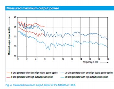
Fig. 4: Measured maximum output power of the R&S®SMA100 B.
Due to the built-in lowpass filters, harmonics suppression of typ. –65 dBc is ensured up to high power levels for all output power options. With its unparalleled combination of very high output power, low harmonics and extremely low wideband noise, the R&S®SMA100 B makes external amplifiers and filters unnecessary, eliminating the need for complicated and expensive test setups.
Rugged and easy-to-use
In automated production environments, it is important to minimize downtime due to servicing and repairs. One typical wear factor in microwave generators has been eliminated in the R&S®SMA100 B: the mechanical step attenuator. For signal generators up to 6 GHz, an electronic (i.e. maintenance-free) step attenuator has been standard for more than a decade. The R&S®SMA100 B is now introducing this technology into the world of microwave generators. Its electronic attenuator, a standard feature, allows very fast and wear-free level settings even at microwave frequencies up to 20 GHz.
The R&S®SMA100 B can be ordered with a size of two or three height units (Fig. 5). Both models come with a touch-operated graphical user interface. The 2 HU instrument saves space in rack installations; the 3 HU model is recommended for laboratory applications due to its larger display and front- panel connectors.
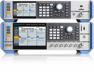
Fig. 5: Slim design for rack applications or with front-panel connectors for the laboratory bench: both models use the same advanced technology.
HIDDEN CHAMPIONS
Internally developed components are the key to building a winner like the R&S®SMA100B
It all started with a (lofty) objective: 10 dB more output power with 10 dB less phase noise and nonharmonics along with much lower harmonic distortion compared with our top model at that time, the R&S®SMA100 A. We wanted the new generator to not only far surpass its predecessor but also to set new standards on the market.
During the first stage in the definition phase, the instrument concept was developed and the key components were identified along with their required specifications. This was a challenge for the design team since at this point the requirements were still often changing, making it necessary to fundamentally modify the concept.
It took intensive market research into component availability and frequent discussions with component suppliers in order to define the requirements for the key components early on and to coordinate the roadmaps of development partners. This was important especially because the long lead times for newly developed ASICs could potentially jeopardize the scheduling of the overall project.
In instances where components classified by Rohde & Schwarz as strategically important are not commercially available with adequate quality, the internal development process is launched. Though the cost of internally developed components is high, there are a number of benefits: besides the customized features, the company has exclusive access to the component and can use it in other instruments with relatively low production costs. Consequently, technology developed for high-end instruments can be transferred in a subsequent stage to medium-priced (or even budget) instruments.
For many years, Rohde & Schwarz has operated a mixed-signal design center staffed by a highly efficient and innovation-oriented team of chip designers specialized in developing key components with performance that exceeds the limits of commercially available products. Rohde & Schwarz collaborates closely with a number of leading semiconductor manufacturers and is able to pick and choose among a wide variety of state-of-the-art semiconductor processes (e.g. GaN or SiGe) to meet technical requirements.
Due to the extremely demanding technical requirements for the R&S®SMA100 B, the company developed numerous key components internally. The most important ones are briefly presented here.
YIG oscillator: As part of a research project sponsored by the Bavarian Ministry of Economic Affairs and Media, Energy and Technology, an entirely new oscillator based on an optimized SiGe transistor was developed in cooperation with the Institute of Microwaves and Photonics (LHFT) at the University of Erlangen-Nuremberg as well as other partners (Infineon AG, Innovent e.V.). Despite its very compact design, this device sets new standards for phase noise across its entire tuning range. For some years now, Rohde & Schwarz has successfully deployed the technology for manufacturing these critical high-quality YIG resonators, and this technology was further developed in cooperation with Innovent e.V. The YIG resonator and transistor are key components in oscillators. Cooperation with our trusted external partners in this research project was the logical next step in further improving the performance of the Rohde & Schwarz YIG oscillators.
Frequency dividers: In order to achieve extremely low phase noise in the synthesizer, a very low-noise oscillator is needed along with high-frequency wideband frequency dividers with very low phase noise and wide- band noise. The company possesses significant expertise in this area based on many years of ongoing development of fast, low-noise divider components. For the R&S®SMA100 B, the company developed a new generation of divider components. An innovative architecture was combined with new circuit concepts implemented using a SiGe semiconductor process to set new standards in the area of phase noise. The performance is 10 dB better than the predecessor modules, thereby surpassing all commercially available components.
Amplifiers: To be able to produce extremely high output power levels ranging up to 10 W in this frequency range, it was imperative to develop new power amplifiers based on the latest GaN technology. This technology can be used to generate power across a very wide frequency range – without having to make compromises in the areas of noise and harmonics. It was also necessary to break new ground with the packaging in order to effectively handle the high dissipated power of the power amplifiers and ensure proper cooling on the printed board.
Switches: Although they are often overlooked, the electronic switches are just as crucial as the high-power amplifiers. Since switches are used to combine the different signal paths at the output of the instrument, they must be capable of handling high power of up to 10 W with very low losses and distortion. Rohde & Schwarz was the first to build these switches based on GaN technology.
The fully electronic 20 GHz step attenuator imposed further requirements on the switches, creating an almost insurmountable problem. In order to implement this module, the switches needed to simultaneously provide very high isolation, low transmission loss, low distortion, very high switching speed and a signal bandwidth of 8 kHz to 20 GHz. In face of the contradictory nature of these requirements, it quickly became clear that not all of them could be satisfied by a single switch design without a substantial loss of instrument performance. The solution involved combining an entirely new step attenuator architecture with various switch topologies and technologies. Different switch structures were developed using CMOS, GaN and AlGaAs technologies to achieve the optimum result for each application. This was the only way to build the first electronic step attenuator for use up to 20 GHz in a signal generator. Without any relay bypass, it delivers very high output power with extremely low harmonic distortion. Such performance was achieved in the past only with mechanical step attenuators. The benefits for the customer are clear: very short setting times without any wear and tear.
Daniel Blaschke, Project Manager RF Signal Generators at Rohde & Schwarz
Jürgen Ostermeier, Director of R&D Microwave Signal Generators at Rohde & Schwar


