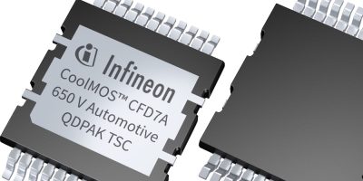
650V CoolMOS CFD7A in a QDPAK meets fast EV charging demands
Addressing the accelerated transition from ICE (internal combustion engine) to EVs (electric vehicles) which demands faster charging systems created using cost-efficient and high performing power electronics, Infineon Technologies has expanded its 650V CoolMOS CFD7A portfolio by introducing the QDPAK package.
This package is designed to provide equivalent thermal capabilities with improved electrical performance compared with TO247 THD devices. This enables efficient energy use in onboard chargers and DC/DC converters, said Infineon.
Efficient and powerful electric vehicle charging systems help reduce charging times and vehicle weight, increasing design flexibility and reduce the total cost of ownership of the vehicle. The 650V CoolMOS CFD7A in QDPAK offers versatility with top-side and bottom-side cooled packages. The QDPAK TSC (top side cooled), enables designers to achieve higher power densities and optimal PCB space utilisation, claimed Infineon.
The 650V CoolMOS CFD7A is constructed for reliable operation in high voltage applications. For example, it has reduced parasitic source inductance, to minimise EMI, ensuring clear signals and consistent performance, said Infineon. There is also the Kelvin source pin which provides improved precision for current sensing, ensuring accurate measurements even in challenging conditions. Another feature is a creepage distance suitable for high voltage applications, as well as high current capability and high power dissipation (P tot) of up to 694W at 25 degrees C.
New system designs using the 650V CoolMOS CFD7A in QDPAK TSC will maximise PCB space use, doubling power density and enhancing thermal management via substrate thermal decoupling. This simplifies assembly, eliminates board stacking and reduces the need for connectors, to lower system costs. The power switch reduces thermal resistance by up to 35 per cent, providing high power dissipation that outperforms standard cooling solutions.
The structure also overcomes the thermal limitations of bottom side-cooled SMD designs using FR4 PCBs, resulting in a significant boost in system performance, claimed Infineon. The optimised power loop design locates drivers near the power switch, improving reliability by reducing stray inductance and chip temperatures.
The QDPAK TSC package has been registered as a JEDEC standard for high power applications, helping to establish a broad adoption of TSC in new designs with a standard package design and footprint. Infineon will also release additional automotive qualified devices in QDPAK TSC for onboard chargers and DC/DC converters in 2024, including 750V and 1200V CoolSiC devices.


