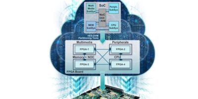
Aldec provides easier access to FPGA-based ASIC and SoC prototyping
Automated design partitioning enables FPGA-based prototyping of SoC or ASIC designs to be reduced in less time says Aldec, at the introduction of HES-DVM Proto Cloud Edition (CE). The design tool is available through Amazon Web Service (AWS), and can “greatly reduce bring-up time” when up to four FPGAs are needed to accommodate a design, says Aldec.
HES-DVM Proto CE can be used with Aldec’s HES pre-silicon prototyping boards, third party boards or platforms users developed in-house. It is available for a monthly license fee, which is practical for use on projects with short prototyping phases. Companies with multiple, simultaneous projects can used HES-DVM Proto CE to evaluate HES-DVM before committing to investing in the traditional licensed version.
HES-DVM’s automatic FPGA partitioning feature allows users to automate the set up of multi-FPGA design prototypes to reduce errors and save time, observed Zibi Zalewski, general manager of Aldec’s hardware division.
Zalewski goes on to say that current SoCs are designed to meet many ASIC type requirements, such as power efficiency, clock distribution, gating and hierarchical bus architecture to assure the highest performance, avoid deadlocks and minimise power demand peaks. “Meeting these many ASIC requirements calls for a design architecture and hierarchy that rarely fits easily into an FPGA-based prototyping platform because of the way resources need to be allocated and interconnections made. Changing the design hierarchy for the sake of the prototyping stage is to be avoided, so it is important to have a tool which will automatically create balanced partitions – picking and placing module instances across the original design hierarchy,” he advised.
The tool should also provide a fine grade of controllability and advanced analysis for timing critical paths or evaluating alternative FPGA partitioning schemes and their impact on interconnections, he added.
It is equally important, he continued, that there is automatic handling of I/O connections with LVDS-based serialisers to resolve issues caused by limited numbers of FPGA I/Os.
“All of the above wishes of designers are met by our HES-DVM . . . Now, HES-DVM Proto CE makes this extremely powerful capability available – at an affordable price and in an easily scalable manner thanks to the ‘on-demand’ cloud operation model – to engineers desperate to reduce their ASIC and SoC design protype bring-up times,” said Zalewski.
HES-DVM Proto CE is delivered as an AWS AMI ready-to-use environment with DVM partitioning software and Aldec’s proven SyntHESer fast synthesis engine. Users need only copy the design RTL source code and can start partitioning immediately, avoiding typical IT or software maintenance issues.
HES-DVM Proto CE can be used for prototypes containing up to four Xilinx FPGAs – present on off-the-shelf prototyping boards like Aldec HES, third party or even in-house-developed FPGA boards that are custom-made for a given project and provide features not available on commercial platforms. If a subsequent revision of the project grows and requires more than four partitions, there is a seamless migration path to the on-premises (standard licensed) version of HES-DVM, which can support any number of FPGAs.


