Consortium announces glass interposer as an SiP
The IoT demands the integration of sensor circuits into application specific integrated circuits (ASICs). ASICs requiring individual packages face quality issues, but a consortium of seven partners from industry and research has developed and characterized a reliable interposer technology as a system in package (SiP) based on glass for broadband millimeter wave modules that can be used in sensors and communication at frequencies above 100 GHz.
“Glass Interposer Technology for Implementing Highly Compact Electronic Systems for High-frequency Applications” (GlaRA) is sponsored by the German Federal Ministry of Education and Research (BMBF – Bundesministerium für Bildung und Forschung). Standard packages do not work because of frequencies are higher than those of mobile communications technology; they exceed 100GHz. They also have stricter environmental requirements. They must allow for adaptation to specialised sensor ASICs and permit manufacturing in medium-sized quantities at competitive prices.
The interposer technology uses various waveguide concepts, high-density micro wiring, and hermetic encapsulation to increase the functions that are able to be integrated. Applications up to 300GHz are possible. The interposer is implemented within a single material system (glass) through waveguide properties and high-precision micromachining, says consortium member, LPKF Laser & Electronics.
The use of glass interposers with electric feedthroughs (vias) provides hermetic packaging which can enclose the components between two glass interposers. The packages are manufactured at wafer level with a diameter of up to 300mm. This allows simultaneous processing of many components and alignment accuracy within the narrow tolerances of RF technology, to reduce costs. Adapted standard systems originally used for machining silicon wafers are employed, which accelerates the technology’s commercial implementation. Glass is also available in large panels, which “considerably” simplifies scaling to large quantities, says LPKF.
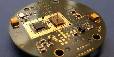
The consortium demonstrated a compact radar front end developed at Endress+Hauser AG for radar fill level sensors, with an operating frequency of 160GHz. The glass package measures just 5.9 x 4.4 x 0.8mm³. It contains a radar ASIC in SiGe technology, all electrical connections to external electronics, test structures for characterisation, and a waveguide connection that can also be used as an integrated primary emitter for a lens antenna. Future fill level sensors will feature high distance resolution, measuring accuracy, and beam focusing at very compact dimensions, says the consortium.
The demos were produced using a new kind of process chain, starting with the laser-induced deep etching (LIDE) from LPKF. The process of generating microstructures in glass prevents damage to the material, which is mandatory for a hermetic glass package. The Fraunhofer Institute for Reliability and Micro-Integration has implemented a process for industrial use for metallising the glass vias with high aspect ratios. A wafer bonding process is used to hermetically package the assembled components by bonding two glass wafers, each of which have vias and cavities.
The conducting paths on the glass substrates are structured and metallised at PacTech. Its SB² laser-supported process is used for the sequential build-up of solder balls. Solder deposits are placed on contact surfaces produced without external current. Different alloys are used to enable staggered assembly at different soldering temperatures. MSG Lithoglas assists with the implementation of the HF packages by producing cavities used to hold the ASIC and other components. High precision spacers made of glass are low temperature coating.
The Institute for Microwave Technology of Ulm University, developed a high frequency concept for the package. The radar signal, in excess of 100GHz, can both illuminate a lens directly via a primary beam and be guided at low loss to a detached antenna via a flexible dielectric waveguide. The different options for emitting radar signals from the package enable a variety of applications.
Sentronics Metrology has developed a 3D high-speed sensor with layer resolutions in the sub-nanometer range for quality control. The sensor has been qualified for detecting leaks in the encapsulated, evacuated glass packages.
The industry partners believe the technology could be used in pressure measurement technology, liquid analysis, photonics, MEMS, medical technology, and communication technology beyond 5G.


