High density source measure unit accelerates semiconductor characterisation
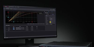
The PZ2100 series is high density precision source measure unit (SMU) that accelerates time to market with flexible software options, said Keysight. It provides 20 precision SMU channels within a 1U rack space to speed the characterisation of IC designs.
Designing a semiconductor component or device and delivering it to market remains a time-intensive, technical process, observed Keysight. Digital development engineers must connect and test multiple ports on a single device under test (DUT) throughout the design cycle to troubleshoot and characterise the performance of the IC. High density, automated characterisation prevents engineers slowing their delivery timelines as they validate with complex, multi-port designs using complicated and low density test setups, the company continued.
The PZ2100 series SMU is scalable to 20 SMU channels in a 1U rack configuration. Cooling spacers are not required when stacked. There are five SMU module options available that are configurable and upgradeable.
Keysight said time is saved by simplifying channel stacking and synchronisation to remove integration and coding complexity. The graphic user interface (GUI) accelerates test prototyping, debugging, and troubleshooting. The PathWave IV Curve Measurement software enables quick measurements and synchronisation without programming.
The all-in-one SMU module also reduces cost by integrating pulser and digitiser functions with conventional SMU functions, such as precise DC voltage and current sourcing and measuring. According to Keysight, it meets emerging requirements without additional instruments.
Keysight specialises in design, emulation, and test solutions to help engineers develop and deploy faster, with less risk, throughout the entire product lifecycle. It serves customers in communications, industrial automation, aerospace and defence, automotive, semiconductor, and general electronics markets.


