
Infineon launches CoolSiC MOSFET 750 V G2 with ultra-low RDS
Infineon has launched its new CoolSiC MOSFET 750 V G2 technology, designed to deliver improved system efficiency and increased power density in automotive and industrial power conversion applications. The CoolSiC MOSFETs 750 V G2 technology offers a granular portfolio with typical R DS(on) values up to 60 mΩ at 25°C, making it suitable for a wide range of applications, including on-board chargers (OBCs), DC-DC converters, auxiliaries for electric vehicles (xEVs) as well as industrial applications in EV charging, solar inverter, energy storage systems, telecom and SMPS.
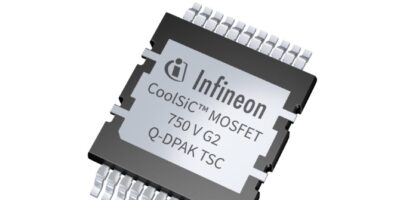
The ultra-low R DS(on) values 4 and 7 mΩ enable outstanding performance in static-switching applications, making the MOSFETs a perfect choice for applications such as eFuse, high-voltage battery disconnect switches, solid-state circuit breakers, and solid-state relays. The best-in-class lowest R DS(on) 4 mΩ is featured in Infineon’s innovative top-side cooled Q-DPAK package, which is designed to provide optimal thermal performance and reliability.
The technology also exhibits excellent R DS(on) x Q OSS and best-in-class R DS(on) x Q fr, contributing to reduced switching loss in both hard-switching and soft-switching topologies with superior efficiency in hard-switching user cases. With reduced gate charge, the technology allows for faster switching and reduces gate drive losses, making them more efficient in high-frequency applications.
Additionally, the CoolSiC MOSFETs 750 V G2 offer a combination of high threshold voltage V GS(th),typ of 4.5 V at 25°C and ultra-low Q GD/Q GS ratio, which reinforce robustness against parasitic turn-on (PTO). Furthermore, the technology allows for extended gate driving capabilities, supporting static gate voltages of up to -7 V and transient gate voltages of up to -11 V. This enhanced voltage tolerance provides engineers with greater design margins and best compatibility with other devices in the market.

