New, robust approach to overvoltage protection for sensitive electronic signal inputs
High demands on the robustness of electronic systems, especially in industrial environments, continually present developers with great challenges. Overvoltage protection is one key design consideration and challenge, as additional components are usually required to protect systems from overvoltage events – yet they frequently impact and, in the worst case, can even falsify signals. Beyond that, these components incur additional costs and contribute to spatial constraints. Hence, when designing the protection circuit, traditional solutions often require a compromise between system accuracy and the protection level.
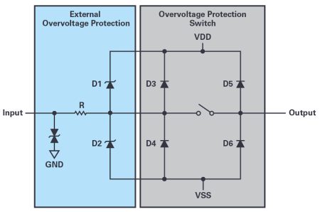
Typically, a common and simple design method uses external protection diodes, usually transient voltage suppressor (TVS) diodes, clamped between the signal line and supply or ground. TVS diodes are advantageous as they can react instantaneously to temporary voltage spikes. This type of external overvoltage protection is shown on the left side of Figure 1.

Figure 1. Traditional overvoltage protection design with additional discrete components.
If a positive transient voltage pulse occurs, it is clamped with a current through diode D1 to VDD. The voltage is thereby limited to VDD plus the diode forward voltage. If the pulse is negative and less than VSS, the same applies with the exception that it is clamped to VSS via D2. However, if the leakage current caused by the overvoltage is not limited, it may damage the diodes. For this reason, there is also a current-limiting resistor in the path. For very harsh environmental conditions, an input-side bidirectional TVS diode is often used for enhanced protection.
The disadvantages resulting from this type of protection circuit appear – for example, in the form of increased edge rise and fall times and capacitive effects. Moreover, it doesn’t provide any protection when the circuit is in the de-energised state.
The actual components, such as analogue-to-digital converters (ADCs), operational amplifiers, etc., usually have integrated protection. This can consist of a switch architecture, as shown on the right side of Figure 1. Figure 1 also shows that input-side and output-side protection diodes are present on both supply rails. The downside to this setup is that, when floating signals appear in a de-energized state (the IC is not powered up), the switch may act as if it is active (even if it is set to OFF) as current will flow through the diodes and the power supply rails. This allows current to pass through, resulting in the signal line losing its protection.
Fault-Protected Switch Architecture
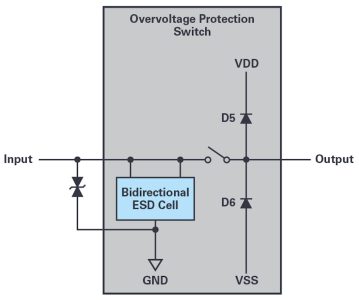
One solution to the challenges mentioned above is a fault-protected switch architecture supplemented by a bidirectional ESD cell, as can be seen in Figure 2. Instead of the input-side TVS diodes, now the ESD cell clamps voltage transients by constantly comparing the input voltage with VDD or VSS. In the case of permanent overvoltage, the downstream switch opens automatically. The input voltage is no longer limited by the protection diodes clamped to the supply rails. The limiting factor is now the maximum voltage rating of the switch. Higher system robustness and reliability are additional advantages. There is also virtually no effect on the actual signals and their accuracy. Moreover, the additional current-limiting resistor is not needed because the leakage currents are very low when the switch is open.

Figure 2. Overvoltage protection with integrated bidirectional ESD cell.
This type of input structure is characteristic of the quad SPST (single-pole, single-throw) switch ADG5412F from Analog Devices Inc. (ADI). This switch permits a permanent overvoltage of up to ±55V, regardless of any existing voltage supply. The ESD cell integrated on each of the four channels clamps voltage transients of up to 5.5kV. In an overvoltage condition, only the affected channel is opened and the other channels continue operating normally.
Conclusion
Thanks to this type of overvoltage protection switches, electrical circuits can be greatly simplified. The advantages over the conventional discrete solution are multitudinous, both in terms of guaranteeing optimal switching performance and robustness in a precise signal chain and in terms of spatial optimisation. Hence, the overvoltage protection offered by the ADG5412F is especially suitable for high precision measurement applications in harsh environments.
About the Author
Thomas Brand began his career at Analog Devices in Munich in 2015 as part of his master’s thesis. After graduating, he was part of a trainee program at Analog Devices. In 2017, he became a field applications engineer. Thomas supports large industrial customers in Central Europe and also specialises in the field of Industrial Ethernet. He studied electrical engineering at the University of Cooperative Education in Mosbach before completing his postgraduate studies in international sales with a master’s degree at the University of Applied Sciences in Constance. He can be reached at thomas.brand@analog.com.


