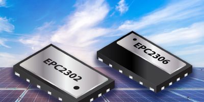
Packaged GaN FETs are in thermally enhanced QFN packages
A packaged GaN FET that is footprint compatible with a previous EPC GaN FET, allowing engineers to make choices to trade off RDS(on) versus price to optimise the design for efficiency or cost by replacing either part number in the same PCB footprint.
The 100V, 3.8 mOhm EPC2306 GaN FET offers high performance and a small size for high power density applications including DC/DC conversion, AC/DC chargers, solar optimisers and micro inverters, motor drives and Class D audio.
The EPC2306 GaN FET has small QG, QGD, and QOSS parameters for low conduction and switching losses. The thermally enhanced QFN package has an exposed top and footprint of just 3.0 x 5.0mm, for the highest power density applications, said EPC.
The EPC2306 is footprint compatible with the previously released 100V, 1.8 mOhm EPC2302. Designers can trade off RDS(on) and price to optimise solutions for efficiency or cost by dropping in a different part number in the same PCB footprint.
“The EPC2306 combines the advantages of 100V GaN with an easy to assemble QFN package without sacrificing performance,” said Alex Lidow, CEO and co-founder of EPC.
The EPC90145 development board is a 100V maximum device voltage, 45A maximum output current, half bridge featuring EPC2306 GaN FET. The board helps developers simplify the evaluation process to accelerate time to market. The 2.0 x 2.0 inch (50.8 x 50.8mm) board contains all critical components for easy evaluation.
All devices and boards are available for immediate delivery from distributor, Digi-Key. Designers can also use EPC’s GaN Power Bench, a cross reference tool which suggests a GaN replacement for silicon MOSFETs.
EPC provides enhancement mode gallium nitride (eGaN) based power management with eGaN FETs and ICs for DC/DC converters, remote sensing technology (lidar), motor drives for e-mobility, robotics, and drones and low-cost satellites.


