PLL/VCO device delivers groundbreaking low phase noise and spur performance
Increasing demands for frequency bandwidth, throughput, and dynamic range in communications systems, together with the need for higher antenna frequencies used in millimetre wave 5G, have all placed further demands on the quality of the local oscillator (LO) or clock used in communications or mixed-signal systems, respectively.
The integrated phase-locked loop (PLL) and voltage controlled oscillator (VCO), the ADF4371, and the similar ADF4372, showcase Analog Devices’ efforts to address the needs of these demanding applications.

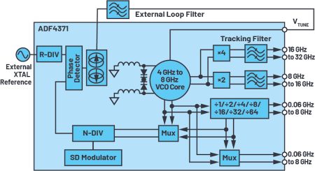
Figure 1. ADF4371 block diagram.
Frequency Coverage
To maximise frequency coverage, the ADF4371/ADF4372 VCO covers an octave range from 4GHz to 8GHz, and, by using frequency dividers at the output, dividing by 1/2/4/8/16/32/64 allows full frequency coverage at the main RF8 output of between 62.5MHz to 8000MHz. A second identical output is provided to allow a user to drive a converter clock. The open-loop VCO phase noise is –109dBc/Hz at 100kHz offset for the 8GHz output frequency.
Until recently, generating high frequencies required the use of external frequency multipliers, typically fabricated on GaAs processes, and they often demanded additional filtering, along with amplification, to overcome the effect of the filtering.
To achieve higher frequencies, the ADF4371/ADF4372 contain an integrated frequency doubler, which provides 8GHz to 16GHz output at the differential RF16 pins. The ADF4371 also features a frequency quadrupler that generates from 16GHz to 32GHz at the RF32 differential output. To minimise the generation of unwanted multiplier products, the ADF4371/ADF4372 contain tracking filters that optimise the power level of the desired frequency while suppressing the unwanted multiplier products. On the doubled output, the VCO feedthrough is –45dBc. On the quad output, the suppression is approximately –35dBc.

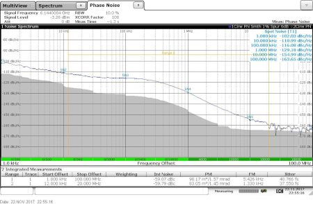
Figure 2. RMS jitter at 6.144GHz.

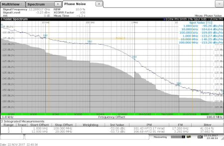
Figure 3. RMS jitter at 12.288GHz.
Leading PLL Performance for Converter Clocks
Improvements to the PLL circuitry mean the ADF4371/ADF4372 devices have a PLL figure of merit (FOM) as low as –234dBc/Hz that, when together with a correspondingly low 1/f noise of –127dBc/Hz (normalised to 1GHz output frequency at 10kHz offset), allows users to generate clocks with an rms jitter number as low as 40fs (1kHz to 100MHz integration limit), making them very suitable for use in the most demanding converter clock applications. A simple low-pass filter with small resistors is recommended in order to minimise the resistor noise, which may appear in the loop. A high frequency (250MHz or 125MHz using the reference frequency doubler) ultralow noise reference source is essential for achieving such low noise. The phase frequency detector (PFD) can operate up to a maximum of 250MHz in integer-N applications. The doubled VCO differential output at RF16 can be used to interface directly to some ADI converters without the need for external balun circuitry, which would increase cost and performance. No degradation in performance from 6.144GHz to 12.288GHz is expected.
Communications and Instrumentation LOs
For wireless and instrumentation applications, the ADF4371/ADF4372 contain 39-bit resolution sigma-delta modulators, which enable frequency generation with sub-millihertz resolution with 0Hz error. In this case, the ADF4371 PFD operates up to a maximum of 160MHz PFD frequency. In these applications, the ADF4371/ADF4372 deliver <48fs rms jitter. The ADF4371 also has industry-leading PLL spurious performance, with PFD spurious as low as –100dBc and in-band, unfiltered integer boundary spurious as low as –55dBc. This performance level greatly simplifies frequency planning and reduces time to market. Many fractional-N PLL and VCO devices have unpredictable fractional-N spurious mechanisms, which can lead to additional unplanned characterisation and frequency planning, which add complexity and cost.
Small Size
The ADF4371/ADF4372 PLL/VCO devices are available in 7mm × 7mm, 48-lead land grid array (LGA) packages. Minimal additional decoupling is required, meaning exceptional performance exists in a small footprint solution.
To achieve the best performance, the use of high quality low dropout (LDO) regulators such as the ADM7150 or LT3045 are recommended. The VCO can be supplied with either 3.3V or 5V, and the remaining circuitry is powered from a 3.3V rail. The ADF4371 can be simulated in ADIsimPLL™ to assist the user in designing the appropriate external component circuitry required to implement a full PLL system.
Conclusion
Industry-leading frequency coverage, performance, and small form factor combine on the ADF4371 to address the high demands of new communication and instrumentation systems.
About the Author
Ian Collins graduated from University College Cork with a degree in electrical and electronic engineering, and he has worked in the RF and Microwave Group at Analog Devices since 2000. He is currently an applications manager in the Microwave Frequency Generation Group, which focuses mainly on phase-locked loop (PLL) and voltage controlled oscillator (VCO) products. When not spending time at work or with his young family, Ian enjoys photography and the theatre (both on- and off-stage), reading, and listening to music. He can be reached at ian.collins@analog.com.


