Zuken updates eCADSTAR for IoT enabled PCB design reuse
Release 2022 of eCADStar makes it easier for design teams to reuse designs, fine-tune high speed circuitry and has a semi-automatic functionality for the layout and modification of densely populated PCB layouts.
The latest release for internet-connected PCB design systems for small and medium-sized businesses presents an internet-connected platform and unified user interface for all applications (schematic, constraint, library and layout editors).
This release sees an emphasis on organisation and reuse of full and partial designs, advanced fine-tuning of high-speed circuitry, and automation-assisted layout and modification of densely populated PCB layouts, said Jeroen Leinders, eCADStar business manager Europe. It is a strong contender for demanding users in the growing market of IoT enabled boards, he added.
This release sees the organisation of large circuit diagrams in eCADStar’s schematic application simplified with the additional support for multi-instanced hierarchy. This makes it possible to group circuit parts (e.g., multi-channels, like amplifiers) that are used several times in a design, into hierarchical blocks. These blocks can be replicated in any number of instances. All instances are updated automatically whenever changes are made to a block definition.
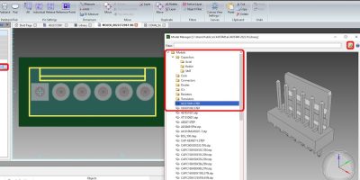
Another enhancement is more structured management of 3D models. A 3D model manager was introduced into the library management. It can import ProStep and other 3D formats. Models can be organised into sub-folders to bring structure and clarity to 3D component models, for example by package, explained Zuken.
Other areas addressed in this release are capabilities for high-speed signals. According to Zuken, a “major overhaul of the configuration editor has made it easier to define or edit physical track and layer stack cross-sections for analysis”. Users can also define etch factors to compensate for impedance variations introduced by inaccuracies in the etching process, either for entire designs or for individual PCB tracks, enhancing accuracy of signal integrity analysis. This feature is particularly useful for high-speed differential signals. For high speed designs, bi-directional cross-probe between the Electrical Editor and the tool’s schematic and PCB has been introduced to relate physical designs to the high-speed equivalent circuits.
Modification of existing layout patterns, such as moving placed components, now supports push-aside, automatically adjusting surrounding components and corresponding routing patterns in real-time. The routing of multi-pad footprint pads, in which single pins correspond to multiple IC pads is now supported.
Component positions can be exported to a CSV file for either an entire layout or part of it. This known good placement can be imported into other designs. This feature is particularly useful for reducing the effort of initial placement through straightforward reuse, as well as for re-using placement of common circuits such as DC/DC converters.


