
3D imaging and metrology system reaches sub micron levels
FocalSpec 3D Line confocal Scanner UULA, the automated optical 3D imaging and metrology system for sub micron level measurements on any material is supported by EyeVision software from EVT.
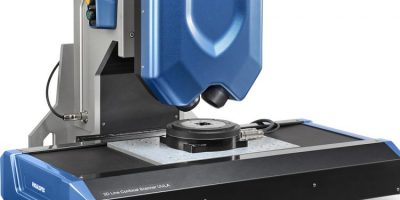
The FocalSpec 3D line confocal scanner UULA is a standalone system used in R&D laboratories, smart manufacturing, and quality control. It is a light source and a CMOS array which are arranged in an angle to each other. The line confocal imaging technology enables customers to model the most demanding surfaces and shapes, even mirror-like, curved and transparent objects. The line confocal imaging sensor detects millions of 3D points per second, and it can distinguish irregularities of less than one micron.
The EyeVision software can carry out different measurements on the captured point cloud and profile. The Metrology command set as well as the 3D Profile commands can be applied to the scans. The Profile Match command can compare previously configured profiles with the scanned profile and therefore can detect defect profiles.
The UULA is designed for devices are becoming smaller and thinner and the materials and shapes designed more complex, explains EVT.
Line confocal imaging laboratory level accuracy is achievable in an industrial environment, confirms the company, with the technology delivering accurate data and high-resolution 3D imaging of metal, glass, paper or plastic surfaces. It also delivers automated, high-speed and high-precision scans of challenging surfaces and shapes, such as mirror-like, curved or multi-layered transparent objects.
The UULA can measure 3D topography and dimensions. It can make tomographic imaging of transparent objects as well as high-precision 2D imaging with extended sharp focus range.
For consumer electronics, the UULA can measure a curved glass display of a smart phone to detect the shape of the glass. It can also measure the gap and offset between the glass and the frame.
For medical devices, it can scan a sheet of printed bio sensors. The 3D dimensions and the surface roughness of the active area can be detected and the thickness of conductive ink can be measured.

