Configurable off-line switcher IC supports USB PD 3.0 + PPS
The latest in the InnoSwitch family of integrated switchers has been announced by Power Integrations. InnoSwitch3-Pro enables digital micro-stepping of voltage and current for precise battery charge control and eliminates DC/DC post-regulators, says the company.
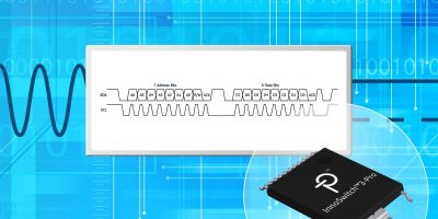
The configurable off-line CV/CC and CP flyback switcher IC is capable of delivering up to 65W and achieving up to 94 per cent efficiency across line and load conditions. Voltage can be controlled in 10mV steps and current controlled in 50mA increments, using the simple two-wire I2C interface. Devices may be paired with a microcontroller or take inputs from the system CPU to control and monitor the off-line power supply. Applications include virtually any rapid-charging protocol, including USB Power Delivery (PD) 3.0 + PPS, Quick Charge 4/4+, AFC, VOOC, SCP, FCP and other industrial and consumer battery chargers, dimmable LED ballast drivers and field-configurable industrial power supplies.
The InnoSwitch3-Pro power-conversion IC includes a microprocessor VCC supply – eliminating the need for an external LDO to power the microcontroller. There is also an n-channel FET driver which may be used to enable or disable the main power output. Together with integrated bus voltage, current and fault-reporting telemetry and dynamically configurable protection functions such as OTP, line OV/UV, output OV/UV, and short-circuit, the bill of materials for an offline power supply, together with design complexity are reduced, says Power Integrations.
The ability to precisely control the output voltage and current of a power supply over a wide range is also useful for designers of specialised applications with smaller production runs, points out the company, as a single board design can eb configured for multiple products using software either at manufacture or during installation.
The InnoSwitch3-Pro IC uses Power Integrations’ high-speed digital communications technology, FluxLink, synchronous rectification, quasi-resonant switching and a secondary-side feedback sensing and feedback control circuit.
Devices are CQC certified, UL recognised and TUV (EN60950) approved to bridge the isolation barrier. The InSOP-24D package is low-profile and thermally efficient, with extended creepage (11.5mm) and clearance between primary and secondary sides for high reliability, surge protection and ESD robustness.
The IC can be used in fast-charging protocols for applications such as smartphones, notebooks, tablets, smart speakers and non-charging applications that require either a load-controlled or configurable output. Samples are available now.


