
Data converter module meets SOSA’s emerging standards
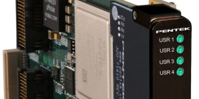
Based on the Xilinx Kintex Ultrascale FPGA, Pentek’s Model 71813 has been added to the Jade family of data converter XMC modules.
The 71813 has 28 pairs of LVDS digital I/O to meet the requirements of emerging standards from The Open Group Sensor Open Systems Architecture (SOSA) Consortium, of which Pentek is a member. The Model 71813 is also claimed to be the industry’s first XMC to implement an optional front panel optical interface supporting four 12Gbits per second lanes to the FPGA.
The module routes 28 pairs of LVDS connections from the FPGA to the XMC P16 connector for custom I/O. When mounted on a compatible single board computer (SBC), the Model 71813 provides a customisable I/O signal status and control interface. In the case of a VPX implementation, the I/O is routed to the backplane where it can handle control and command signals to the chassis being defined in the evolving SOSA initiative.
The Model 71813 can be optionally configured with a front panel, multi-fibre push on (MPO) optical connector for supporting four lanes of 12Gbits per second to the FPGA. With user-installed FPGA IP, the Model 71813 can be used as an optical interface for 10GigE, 40GigE, Aurora or custom protocols, adds Pentek.
The combination of the Xilinx Kintex Ultrascale FPGA, LVDS digital I/O and optical I/O, result in a high performance off-load co-processor to fit an assortment of processing needs in the most demanding of applications, confirms Pentek.
The Model 71813 is already being used by Kontron, a leading global provider of IoT/embedded computing technology, with its new VX305C-40G 3U VPX SBC. The SBCs were developed in line with the SOSA technical standard and designed specifically to meet the needs of the US militarty for Open System Architecture (OSA) computing platforms.
The Pentek Jade architecture is based on the Xilinx Kintex UltraScale FPGA, which raises the digital signal processing (DSP) performance by over 50 per cent while reducing cost, power dissipation and weight, says Pentek. The PCI Gen.3 interface allows access to control and status registers for controlling algorithms, state machines and data flow across the LVDS SOSA I/O port and the optional front panel optical port. A 5Gbyte bank of DDR4 SDRAM is available for additional functions. The factory-installed DMA controller can sustain 6.4Gbytes/s data transfers across PCIe.
Pentek’s Navigator Design Suite was designed for the Jade architecture and Xilinx’s Vivado Design Suite for IP and control software creation and compatibility. Graphical design entry for Xilinx and Pentek AXI4-compliant IP modules using the Xilinx IP Integrator are claimed to speed development tasks. The Navigator Design Suite consists of the Navigator FPGA design kit (FDK) for integrating custom IP into Pentek sourced designs and Navigator board support package (BSP) for creating host applications. Users can work at the API level for software development and with an intuitive graphical interface for IP design. The Navigator BSP is available for Windows and Linux operating systems.

