
Inline inspection for PCBs uses 2D line scan technology
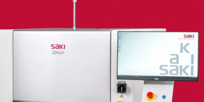
Saki will be introducing its 2Di-LU1 inline bottom-side automated optical inspection (AOI) system at Nepcon China, Shanghai, China, and SMTconnect, Nuremberg, Germany. The 2D line-scan technology captures the image of a 460 x 500mm PCB assembly (PCBA) and carriers measuring 610 x 610mm in one pass and in real time. The image is stored to memory and inspection data is created for the entire board. The system automates the bottom-side inspection process, eliminates board flipping and handling, and ensures quality after the potting, dip, wave, and selective soldering processes.
The 2Di-LU1 software includes Saki’s proprietary Fujiyama algorithm, which provides through-hole joint inspection in a single step. It simultaneously inspects for copper exposure, pin detection, pin-holes, solder fillet abnormalities, missing components, soldering problems and bridges. The company’s inspection software has been used for extra component detection of solder balls and foreign objects and through-hole device inspection in the automotive industry for several years and complies with the IPC-A-610 standard.
The 2Di-LU1 bottom-side AOI system is based on Saki’s rigid, time-tested hardware that ensures stable machine performance and long hardware life. The system supports L-size PCBs, high clearances, heavy substrates, and mounted jigs, adds Saki.
Visitors to Nepcon China (24 to 26 April) can see the 2D bottom-side AOI system, 3D AOI, SPI, and AXI systems and Saki Self-Programming Software, at the Saki booth 1J30 and the Fuji booth 1G60. The company will also be at SMTconnect (7 to 9 May) Hall 4A-133.
Since 1994, Saki has specialised in the development of automated recognition through robotic vision technology. The company’s 3D automated solder paste, optical, and x-ray inspection systems (SPI, AOI, AXI) enable M2M communications, improve production and process efficiency.

