
Innoscience develops SolidGaN integrated half bridge with driver
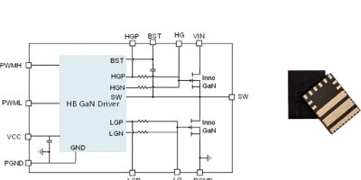
GaN-on-Si HEMT manufacturer, Innoscience Technology, has developed an integrated half bridge and driver. The ISG3201 is the first in a family of SolidGaN integrated GaN devices. It is a complete half bridge circuit and includes two 100V 3.2 mOhm InnoGaN HEMTs (high electron mobility transistor) and the required driver circuitry in an LGA package. Dimensions are just 5 .0 x 6.5 x 1.1mm.
According to Yi Sun, general manager of Innoscience America, the addition means that the company offers designers a choice between the flexibility of using a discrete solution and an integrated approach which is “very compact and simple to use and soldering and simplifying the power stage layout”.
The ISG3201 SolidGaN half bridge comprises two 100V 3.2 mOhm e-mode GaN HEMTs with driver, driving resistor, bootstrap and Vcc capacitors. It has a 34A continuous current capability, zero reverse recovery charge and low on resistance. The high level of integration ensures that the gate loop and power loop parasitics are kept below 1nH, explained Innoscience. As a result, voltage spikes on switching nodes are minimised. The turn on speed of the half bridge GaN HEMTs can be adjusted using a single resistor.
The ISG3201 is suitable for high frequency buck converters, half bridge or full bridge converters, Class D audio amplifiers, LLC converters and power modules. Innoscience estimates that the ISG3201 can save up to 20 per cent PCB space on discrete GaN designs and 73 per cent board space on traditional silicon implementations.
The company plans to introduce more SolidGaN integrated GaN-based products this year, including further half bridge circuits with different voltage ratings.
Innoscience is an integrated device manufacturer (IDM) founded in December 2015 with investment from CMBI, Arm, SK and other investors. Its vision is to create an energy ecosystem with effective and low cost GaN-on-silicon (GaN-on-Si) power devices.
In November 2017, Innoscience established a mass production eight-inch wafer line for GaN-on-Si devices in Zhuhai, China. It opened a new facility in the Suzhou in September 2020.
Innoscience’s GaN power devices can be used in diverse applications including cloud computing, electric vehicles (EV) and automotive, portable devices, mobile phones, chargers and adapters.

