
PCIe board based on RFSoC targets wireless applications
Expanding the Quartz RFSoC architecture family, Pentek announces the Model 7050. This eight-channel A/D and D/A converter, PCIe double-wide board is based on the Xilinx Zynq UltraScale+ RFSoC.
According to Pentek, the Model 7050 brings RFSoC performance to PC platforms with a complete system on a board. The Zynq UltraScale+ RFSoC FPGA is the industry’s only single-chip, adaptable radio platform and is popular for 5G and LTE wireless, SIGINT and COMINT, EW countermeasures, radar on a chip, test and measurement, satellite communications and lidar applications.
The PCIe form factor makes it easy to develop or deploy on a standard desktop PC and the Pentek software, developed on the PCIe board, can be moved seamlessly to other form factor platforms, including VPX and custom small form factor (SFF), explains Pentek.
All control and data paths on the Model 7050 are accessible by the RFSoC’s programmable logic and processing system. A full suite of Pentek-developed IP and software functions use this architecture to provide data capture, timing and interface solutions for many of the most common application requirements.
The Pentek Quartz architecture simplifies the design to reduce power and cost, while still providing some of the highest performance FPGA resources available today, claims the company. It is designed to work with Pentek’s Navigator design suite tools to develop and deploy software and FPGA IP for data and signal processing.
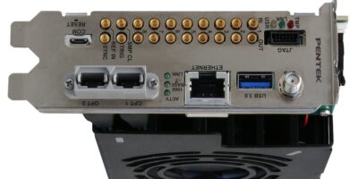
The Xilinx Zynq UltraScale+ RFSoC processor integrates eight RF-class A/D and D/A converters into the Zynq FPGA fabric and quad Arm Cortex-A53 and dual ARM Cortex-R5 processors, creating a multi-channel data conversion and processing solution on a single chip. The Quartz board architecture adds 16Gbytes of DDR4 SDRAM, clocking for single board and multi board synchronisation, high-signal integrity connectors for RF inputs and outputs, x8 PCIe Gen 3 interface, an eight-lane, 28Gbits per second optical interface with industry standard MPO connectors for supporting gigabit serial protocols. There are also 12 LVDS general purpose I/O pairs for specialised interfaces, an on-board GPS receiver and factory-installed application IP.
Modules include DMA engines, DDR4 memory controllers, test signal and metadata generators, data packing and flow control. The board is pre-installed with IP for triggered radar chirp generator, triggered radar range gate engine, wideband real-time transient capture, flexible multi-mode data acquisition and extended decimation. The Model 7050 can be used out-of-the-box with the built-in functions requiring no FPGA development, explains Pentek.
The front end accepts analogue IF or RF inputs on eight panel mounted MMCX connectors with transformer-coupling to eight four Gsamples per second 12-bit A/D converters delivering either real or complex DDC samples. With additional IP-based decimation filters, the overall DDC decimation is programmable from two to 128. The eight DACs accept baseband real or complex data streams from the FPGA’s programmable logic. Each 6.4Gsamples per second 14-bit D/A includes a digital upconverter with independent tuning and interpolations of one, two, four and eight. Each D/A output is transformer-coupled to an MMCX connector.
Pentek’s Navigator Design Suite includes Navigator FDK (FPGA Design Kit) for custom IP and Navigator BSP (Board Support Package) for creating host software applications.

