
Pentek expands Jade family with RF tuner based on Xilinx’s Kintex UltraScale
XMC FPGA modules from Pentek now include the Jade Model 71891. The L-Band RF tuner has two 400MHz A/Ds based on the high density Xilinx Kintex UltraScale FPGA. The module is designed for connection directly to SatCom or communications system L-band signals.
The upgrade to the Jade Architecture increases performance while reducing power by 20 per cent and lowering cost by 35 per cent, said Bob Sgandurra, director of Product Management for Pentek. “The Navigator Design Suite also provides them with a more robust toolset and extensive library of IP resources,” he added.
The module has a front panel SSMC connector which accepts L-Band signals between 925 and 2175MHz, typically from an L-Band antenna or an LNB (low noise block). The Maxim MAX2121 tuner, with a programmable low noise amplifier (LNA), directly converts the L-Band signals to IF or baseband using a broadband I/Q analogue down converter and then by 123MHz low pass anti-aliasing filters. The two analogue tuner outputs are digitised by two ADS5474 400MHz, 14-bit ADCs from Texas Instruments which capture the full 123MHz bandwidth.
The analogue outputs of the MAX2121 can be used in the IF mode instead of the analogue baseband I+Q mode. In this case, each ADC digitises an IF signal and then delivers it to a DDC to produce perfectly balanced complex I+Q digital baseband samples for enhanced demodulation performance. An additional benefit of using the IF analog output mode is that two independent A/D and direct DC (DDC) channels are now available for digitising and down converting two signals with different centre frequencies and bandwidths.
The Model 71891 features two acquisition IP modules to capture and move data. Each module can receive data from either of the two ADCs or a test signal generator. Each acquisition IP module contains a powerful DDC IP core with decimation values from two to 64k, covering a wide range of signal bandwidths. Because of flexible input routing within the acquisition IP modules, different configurations can be achieved including one ADC driving both DDCs or each of the two ADCs driving its own DDC.
The Pentek Jade architecture is based on the Xilinx Kintex UltraScale FPGA, which raises digital signal processing (DSP) performance by over 50 per cent over the previous family, reports Pentek. There are also “equally impressive reductions in cost, power dissipation and weight” according to the company. The FPGA has access to all data and control paths, enabling factory-installed functions including data multiplexing, channel selection, data unpacking, gating, triggering and memory control.
Pentek’s Navigator Design Suite includes Navigator FPGA Design Kit (FDK) for custom IP and Navigator board support package (BSP) for creating host software applications.
The Navigator FDK includes the board’s entire FPGA design as a block diagram that can be graphically edited in Xilinx’s Vivado tool suite, with full source code and documentation. Developers can integrate their IP along with the factory-installed functions or use the Navigator kit to replace the IP with their own. The Navigator FDK Library is fully AXI-4 compliant, providing a well-defined interface for developing IP or integrating IP from other sources.
Pentek’s Navigator BSP provides a full suite of high-level C-callable libraries that support all features of the Model 71891 and demonstrate all of its functional modes with examples. The software package is provided with complete source code allowing the user to modify and integrate this functionality into the end application.
Navigator BSP also includes a Signal Viewer utility that allows developers to view digitised signals from the output samples of any DDC in time and frequency domain.
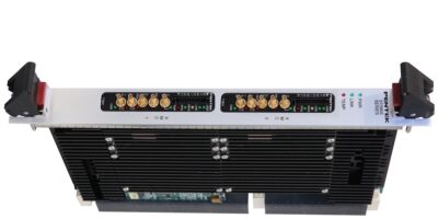
The Jade Model 71891 XMC is designed for commercial, rugged or conduction cooled operating environments. It is also available packaged in several form factors, including 3U and 6U VPX (Models 54891 and 57891/58891); 3U and 6U cPCI (Models 72891/73891/74891); AMC (Model 56891); and PCIe (Model 78891). Additional FPGA, A/D and LVDS FPGA I/O options are available. Delivery is eight weeks from receipt of order.

