
Plating tool supports wafer-level packing in compound semiconductors
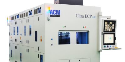
Adding to the wafer processing options for semiconductor and wafer-level packaging (WLP) applications available from ACM Research, the Ultra ECP GIII plating tool supports WLP for compound semiconductors, including silicon carbide (SiC), gallium nitride (GaN) and gallium arsenide (GaAs).
The tool is also capable of plating gold (Au) into back of board, deep hole processes with greater uniformity and better step coverage, said ACM. The fully automated Ultra ECP GII supports high volume manufacturing that accommodates both flat and notched six-inch wafers.
“The compound semiconductor market is growing rapidly with strong demand from electric vehicles, 5G communication, and RF and AI applications,” said David Wang, ACM’s chief executive officer and president. “Historically, compound semiconductor manufacturing processes have seen limited levels of automation, and have been subject to restricted production volumes. Further, most plating has been performed by vertical-type plating tools with poor uniformity performance,” he explained.
The Ultra ECP GIII plating tool overcomes these challenges using ACM’s second anode and ACM’s paddle technologies. Second anode technology effectively tunes wafer-level plating performance to overcome issues created by electrical field distribution differences. It can be used to optimise big die at wafer edge area patterns and notch area to achieve plating uniformity within three per cent.
Paddle technology achieves stronger agitation to enhance mass transfer, resulting in significantly better step coverage in deep holes, said ACM. Improved step coverage enables a reduction in Au (gold) film thickness, achieving cost savings.
Compound semiconductor manufacturers can use the plating tool to support wafer level packaging with copper–nickel–tin-silver plating modules using second anode technology, integrated with a vacuum pre-wet chamber and a post-clean chamber, or for Au plating systems.
ACM Research develops, manufactures and sells semiconductor process equipment for single-wafer or batch wet cleaning, electroplating, stress-free polishing and thermal processes critical to advanced semiconductor device manufacturing as well as wafer-level packaging. The company is committed to delivering customised, high-performance, cost-effective process solutions that semiconductor manufacturers can use in numerous manufacturing steps to improve productivity and product yield.

