
Power integrity and its impact on signal integrity
The trend is ongoing: Newly developed electronic circuits must support higher data rates with increasingly tiny circuit dimensions, all the while consuming less power. As a consequence, development engineers are faced with major challenges and the subject of power integrity is becoming increasingly important.
Higher data rates are a driving force behind the increasing quality requirements for clock and data signals. In order to achieve lower power consumption, chipsets are now used with smaller and smaller supply voltages. The actual supply voltage must be free of interference and conform to increasingly stringent tolerance limits so that the signals generated by the chipsets can satisfy the demanding signal integrity requirements. This is why the subject of power integrity is growing in importance.
Power integrity involves ensuring a high-quality supply voltage. For electronic circuits, the relevant supply voltages are almost exclusively DC voltages. An oscilloscope with the appropriate accessories is generally used to make these quality measurements. The oscilloscope must be capable of displaying the supply voltages with high resolution and extremely low inherent noise.
Ideally, the DC supply voltages should be constant with zero noise. In reality, however, they always exhibit a certain amount of ripple and superimposed noise. Understanding why this is the case requires a look into the design of the supply voltage network.
Typically, the source of a supply voltage network (e.g. an AC/DC power supply or a battery) provides the on-board voltage. The on-board voltage is a DC voltage with common voltage levels such as 12 V or 5 V. This primary supply is then used to feed the necessary voltages and currents to all of the active components. However, since different components need different voltages, we might commonly encounter 10 to 20 different voltage levels. What this means for the developer is that the given on-board voltage must be adapted for every component. Highly efficient switching regulators are generally used for this purpose. One disadvantage of switching regulators compared to less efficient linear regulators is that the DC voltage is corrupted during the regulation process and periodic noise is superimposed on the DC signal. This residual noise is known as ripple.
During conversion of the voltage levels, random (nonperiodic) disturbances, which are generically categorized as noise, occur in addition to the ripple. The major contributors here are the noise of the voltage source and the noise produced by the switching currents flowing in the supplied circuit. Other relevant components include the thermal noise as well as interference from nearby circuits.
In addition to these disturbances and interference related to the switching regulation and design, we should also analyze the dynamic behavior. Sudden changes in the load current (e.g. due to a microcontroller changing state from idle to busy) can cause a momentary drop-off in the supply voltage. Just like the ripple and noise, this drop-off must not exceed the limits specified by the manufacturer, i.e. it must be regulated within an acceptable time interval.
The DC accuracy is another key characteristic for voltage supplies. Here, two parameters are relevant: the absolute voltage level and the long-term stability of the voltage level.
In order to ensure that all of the discussed parameters fall within the specified limits, it is important to verify these parameters using suitable T&M equipment during the development process.
Growing T&M challenge
The requirements for measuring noise, ripple, dynamic behavior and DC accuracy have increased sharply in recent years. Some reasons why the supply voltage levels for the different components are decreasing include growing integration density on chips and the smaller dimensions needed to achieve this integration density. Naturally, there is also the design objective of lower power consumption. In parallel, the permissible tolerances for ripple and noise have also been significantly reduced by the chip manufacturers. This trend means that the interference signals that need to be measured have lower and lower levels. The technical challenge faced by the measuring system (oscilloscope and probe) is growing because the inherent noise of the measuring system is often as high as the interference signals to be measured. This noise is superimposed on the signal being measured and can make the result appear much worse than it really is. Under certain circumstances, this can cause a tolerance violation to be triggered that is not actually present (see Fig. 1).

Fig. 1: Influence of noise and drift on the measurement result.
Another important issue is that an inadequate voltage offset is often set on the oscilloscope, which means the optimum vertical resolution is not fully utilized. This produces a further increase in measurement uncertainty. Possible solutions include using the oscilloscope’s AC mode or inserting a DC blocker. However, this causes the information about the DC voltage component to be lost, meaning any slow drift cannot be detected. In order to be certain upon completion of the measurement that the DC voltage, including any drift, ripple and noise, is within the specified tolerance, it is essential to use a high-performance measuring system.
Signal analysis in the frequency domain
Most of the solutions that are available for this type of measurement are based on an oscilloscope combined with special probes. The probes are typically active and have a duty cycle of 1:1 along with very low inherent noise. To compensate for the DC voltage level, they have a built-in offset voltage source. The adjustable offset voltage can range up to ±60 V, depending on the manufacturer. The bandwidth of the latest commercially available probes is 2 GHz or higher. Even high frequency interference coupled by nearby signals (e.g. 5 Gbit/s data line, 2.4 GHz Wi-Fi signal) can be detected. Coupled signals of this kind generally have low levels, making it nearly impossible to find or analyze them in the time-domain signal. In such cases, analysis in the frequency domain can be very beneficial. Using the oscilloscope’s FFT function, this kind of interference is easily detected. Moreover, the source of the interference can often be localized by analyzing its frequency.
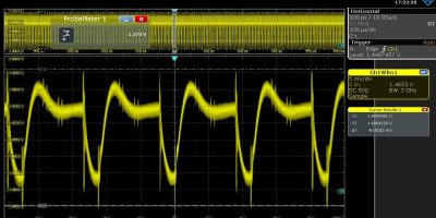
After analyzing the signal in terms of ripple and noise, there are other challenges related to measuring the DC accuracy. As tolerances become more stringent, the absolute DC level must be measured with great precision. However, this measurement is problematic with an oscilloscope due to the fact that the signal tapped by the probe is normally converted into an 8-bit signal in the oscilloscope. Assuming a vertical setting of 200 mV/division and 8-bit conversion, accuracy of 6.25 mV is obtained. With a tolerance band of, say, 30 mV, this implies uncertainty of greater than 20 % that must be taken into account. The ideal solution is a probe with an integrated voltage meter (probe meter; see Fig. 2). The integrated voltmeter is based on a 16-bit converter. This makes it possible to determine the voltage with 256 times greater precision compared to a probe without this feature.

Fig. 2: Voltage ripple and precision measurement of the DC voltage using a probe meter (16-bit ADC).
Noise and ripple are performance-impairing
Noncompliance with the specified levels and tolerances can impair the functioning of the entire system. A simple example of this problem involves a microcontroller that is reset and restarts during a change of load due to an excessively deep and long-lasting voltage drop-off. Faulty behavior of this kind should be obvious, making it relatively easy to track down and correct. However, this is not the case if the system does not crash immediately, meaning the “only” result is a degradation in signal quality combined with sporadic occurrence of errors. Modern electronic circuits contain a number of active components which can cause problems if a “faulty” supply voltage is provided.
Voltage-controlled oscillators (VCO) are critical components nowadays. Being subject to stringent requirements, they require a very high-quality voltage supply. Excessive ripple or noise on the voltage causes increased phase noise in the output signal. When integrated in a PLL or a clock generator, this interference is propagated, thereby causing increased jitter in the clock signal or instability in the PLL. For example, if an analog-to-digital converter (ADC) is supplied with a clock signal that has jitter, bit errors can arise in the conversion process. As a result, sensor values will be incorrectly converted and processed.
These examples have demonstrated the close relationship between signal integrity and power integrity. Inadequate consideration of issues related to power integrity (or inaccurate measurements) can lead to problems in the area of signal integrity. This can necessitate time-consuming and costly redesign of a faulty product along with delays in the market introduction process. As a result, it is important to consider these issues and perform appropriate verification measurements with great care.
Thomas Rottach, Market Segment Manager Focus Digital Design & Power Electronics
Rohde & Schwarz GmbH & Co. KG,

