
Prototyping platform delivers digital twin checks
A universal signal processing architecture (USPA) prototyping platform announced by Keysight Technologies enables semiconductor companies to conduct complete chip prototyping and verification, pre-tapeout, in a real-time development environment integrating digital twins of fully-compliant, standards-based signals.
The silicon tapeout stage in the chip design process is an increasingly expensive procedure and one that leaves little room for design failure. If a design fails following the tapeout, chip makers must start over again with a re-spin that can take 12 months or longer to complete. In addition to tying up valuable research and development resources, these chip redesigns can potentially cause the chip maker to miss a narrow time-to-market window.
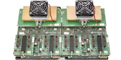
To reduce the risks of design failures and expensive re-spins, the Keysight USPA platform provides chip designers and engineers with complete digital twin signalling to verify designs before they are committed to silicon. The USPA platform offers designers an alternative to proprietary custom prototyping systems by integrating fast signal converters with a high performance, modular FPGA prototyping system.
Benefits of the USPA prototyping platform include support for high performance optoelectronic development projects with DAC and ADC interfaces that emulate signals at full speed, up to 68Gsamples per second (ADC) and 72Gsamples per second (DAC).
It also provides a broad range of input / output interfaces that are suitable for applications including 6G wireless development, digital radio frequency memory, advanced physics research and high-speed data acquisition applications, such as radar and radio astronomy.
It is available as a pre-configured system for single channel transceiver applications and as a fully configurable set of modular components that can be combined to support a range of single and multi-channel applications. The pre-configured system can be expanded with additional components to optimise the scalability and cost-effective reusability of the platform architecture, said Keysight.
Dr. Joachim Peerlings, vice president and general manager of Keysight’s network and data centre group, said: “By accelerating and de-risking chip development, Keysight USPA delivers a new end-to-end solution that meets the challenges of leading-edge designs in a very high-cost environment. This powerful platform gives chip developers a digital twin of their future silicon device, allowing them to fully validate their designs and algorithms before incurring the expense and risk of a tapeout.”

