Substrate coupling analysis tool is upgraded to include BCD-on-SOI process
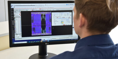
X-Fab Silicon Foundries SE has expanded the scope of its SubstrateXtractor tool, used for the examination of unwanted substrate coupling effects. X-Fab claims to be the first foundry to offer this analysis function for a BCD-on-SOI process.
The tool was originally designed for the XH018 and XP018 180nm bulk CMOS processes, which it still supports. Using the SubstrateXtractor version, accelerated SOI-related product development can be achieved, avoiding the need for multiple iterations, says the company.
The initial SubstrateXtractor was developed in collaboration with EDA partner PN Solutions (and is based on its PNAware product). Customers address the coupling issues caused by interactions between active and passive elements within semiconductor substrates (whether these elements are part of the circuit itself or present parasitically). Support for SOI processes is built on the PNAwareRC tool.
The BOX/DTI features of X-Fab’s XT018 process enable isolation of constituent functional blocks on the chip. This can apply to sensitive analogue blocks needing to be decoupled from digital blocks, or low noise amplifiers that must be isolated from high voltage driver circuits. It also makes multi-channel implementations much easier, as circuits in XT018 are effectively placed in their own separate substrate, thereby reducing crosstalk.
SubstrateXtractor can analyse substrate couplings in SOI-based ICs. While active silicon islands in SOI processes can be completely dielectrically isolated by BOX and DTI, passive R and C couplings may still be present. The updated tool extracts a passive RC network for lateral and vertical coupling paths resulting from DTI and BOX. These passive coupling networks can be simulated, in order to assess what impact they will have on the IC.
Key applications for this additional post-layout extraction will be the high-current and high-voltage devices used in industrial and automotive systems.
X-Fab is an analogiue/mixed-signal and MEMS foundry group manufacturing silicon wafers for automotive, industrial, consumer, medical and other applications. X-Fab’s modular CMOS and SOI process geometries range from 1.0 micron to 130nm. It also has SiC (silicon carbide) and MEMS long-lifetime processes. X-Fab’s analogue-digital ICs (mixed-signal ICs), sensors and MEMS are manufactured at six production facilities in Germany, France, Malaysia and the US.

