binder prints electronics functions directly onto the component
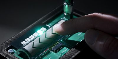
binder has developed a process for printing electronic functions directly onto the surface of components, enabling sensors, heating elements and conductive tracks to be integrated without the need for separate circuit boards or additional assemblies.
Developed at the company’s Innovation and Technology Centre (ITZ) in Bad Rappenau, the technology uses high-precision screen and pad printing to deposit conductive and dielectric materials onto plastic, metal, glass and ceramic substrates. The process can also be applied to curved and three-dimensional surfaces that are difficult to accommodate using conventional PCB technology.
By integrating electronic functions directly into the component, manufacturers can reduce the number of individual parts, save installation space and simplify assembly while increasing design flexibility.
Potential applications include printed sensors for condition monitoring and predictive maintenance, touch and force sensors for user interfaces, and integrated heating elements for temperature control. The technology is particularly suited to compact devices where space is limited.
The printed electronics are developed at binder’s ITZ before being transferred to binder solutions for customer-specific implementation. The company combines the printed functional layers with its existing expertise in connectors, cable assemblies, precision-turned parts and zinc die-cast components to produce complete assemblies.
The approach allows functional prototypes to be developed into production-ready components, providing a route to integrating sensing, heating and electrical interconnects directly into next-generation electronic products.

