
Thin film, short wave infrared image sensor exceeds InGaAs-based versions
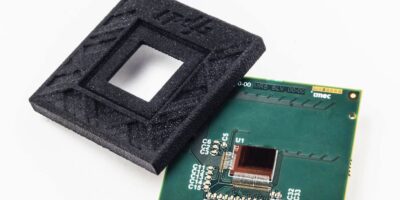
A prototype, high resolution, short wave infrared (SWIR) image sensor with record small pixel pitch of 1.82 micron is based on a thin film photodetector that is monolithically integrated on a custom Si-CMOS readout circuit. The prototype has been developed by imec and uses a fab-compatible process flow, in preparation for high throughput, wafer level manufacturing. The research technology largely exceeds the capabilities of today’s InGaAs-based SWIR imagers in terms of pixel pitch and resolution, says imec, with disruptive cost and form factor potential. New applications are enabled, even in cost-sensitive domains, such as in industrial machine vision, smart agriculture, automotive, surveillance, life sciences and consumer electronics, continues the research group.
Sensing in the short wavelength infrared (SWIR) range (i.e. wavelengths from 1400nm to above 2000nm) offers advantages over the visible (VIS) and near-infrared (NIR) range for some applications. SWIR image sensors can, for example, see through smoke or fog, or even through silicon, making them practical for inspection and industrial machine vision applications. To date, SWIR image sensors are produced through a hybrid technology, in which a III-V-based photodetector (usually InGaAs-based) is flip-chip bonded to a silicon readout circuit. These sensors can be sensitive, but the technology is expensive for mass manufacture and limited in size of pixel and number of pixels.
Imec’s alternative enables record small sub-2 micron pixel pitch, by monolithically integrating a thin film photo detector stack with a Si-CMOS readout circuit. The photo detector pixel stack implements a thin absorber layer such as 5.5nm PbS quantum dots, which corresponds to peak absorption at 1400nm wavelength. The peak absorption wavelength can be tuned by adjusting the nanocrystal size and is extendable to wavelengths even above 2000nm. At the peak SWIR wavelength, an external quantum efficiency (EQE) of 18 per cent is obtained (and can be upgraded towards 50 per cent with further improvements). The photo detector stack is monolithically integrated with a custom readout circuit, processed in 130nm CMOS technology. In this readout circuit, the three-transistor pixel design was optimised for the scaling of pixel size in the accessible 130nm technology node, resulting in a pitch of 1.82 micron for the prototype SWIR imager.
The image sensors can be deployed in industrial machine vision (e.g. photovoltaic panel monitoring), smart agriculture (e.g. inspection and sorting), automotive, surveillance, life sciences (e.g. lens-free imaging) and many more. The small form factor means it could be integrated in small cameras in smartphones or AR/VR glasses – with eye-safe SWIR light sources.
The prototype SWIR image sensor was developed in imec’s Pixel Technology Explore research program.

